

Top
Author
Published
11 Apr 2024Form Number
LP1932PDF size
5 pages, 511 KBSubscribed to LP1932.
Thank you for your feedback.
Abstract
Semiconductor chips are a significant component of almost every product, from autos to aircraft to medical devices. Today’s semiconductor chips are incredibly complex, can contain over one billion circuit elements, and are expensive to produce. By partnering with AMD, Lenovo provides manufacturers with a high-performance infrastructure for EDA to mitigate these high costs/risks, handle larger designs, and improve time-to-market, innovation, simulation accuracy, and parallel processing efficiency.
Introduction
For several decades, semiconductor design and manufacturing companies have been using EDA tools to:
- Design and validate the manufacturing process to ensure it delivers semiconductor chips with the required performance, density, quality, and yields.
- Verify that a chip design meets functionality, reliability, and performance requirements.
- Monitor the performance throughout the silicon lifecycle from post-manufacturing test to field deployment and operation.
EDA workloads consist of two high-level design phases (Figure 1) with a mix of sequential and threaded codes that are highly compute-intensive. The Front-End Design phase mainly has small files, which are more dominant. The Back-End phase typically has large files. Verification and regression usually consume most of the computing capacity.
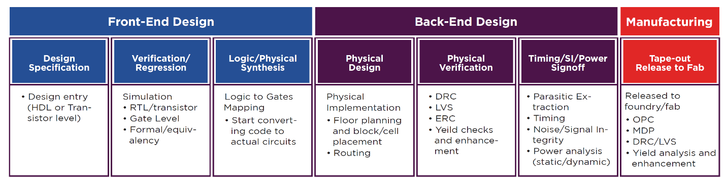
Figure 1. The EDA Workflow
Today’s semiconductor chips are incredibly complex and can contain over one billion circuit elements, all interacting with each other in subtle ways and highly sensitive to minor variations in the manufacturing process. Projects must be error-free before tape-out to mitigate the high costs of committing a design to silicon.
To manage this level of complexity, sophisticated automation with EDA on a high-performance infrastructure is critical for:
- Faster Time-to-Market: Accelerate complex EDA tasks, such as simulation, verification, and synthesis, to iterate through design cycles quicker, ultimately reducing time-to-market for new products and gaining competitive advantage.
- Innovative Design Exploration and Optimization: Explore a broader range of design options and parameters, leading to the discovery of improved and optimized product designs.
- Handling Larger Designs: Work on advanced technologies and more intricate integrated circuits.
- Parallel Processing for Efficiency: Designers can parallelize many EDA tasks to take advantage of large core counts that significantly improve efficiency and computational throughput.
- Improved Simulation Accuracy: More detailed and precise simulations are crucial for ensuring the reliability and performance of semiconductor devices.
Consequently, the use of EDA in semiconductor manufacturing can be essential.
EDA Benefits Beyond the Electronics Industry
However, EDA use is not just confined to the electronics industry. Semiconductor chips and systems are significant components of autos, aircraft, and medical devices. The modern car is essentially a computer on wheels. It is designed and developed with many computer-aided design/engineering (CAD/CAE), EDA, augmented/virtual reality (AR/VR), and artificial intelligence/machine learning (AI/ML) tools working together to create a digital twin (Figure 2). A digital twin is a digital replica, or “twin,” of a physical object or business process. Digital twins can be digital replicas of real components, systems, factories, cities, or even the entire planet. These interdisciplinary simulations drive more EDA growth and require a cost-effective, high-performance infrastructure.
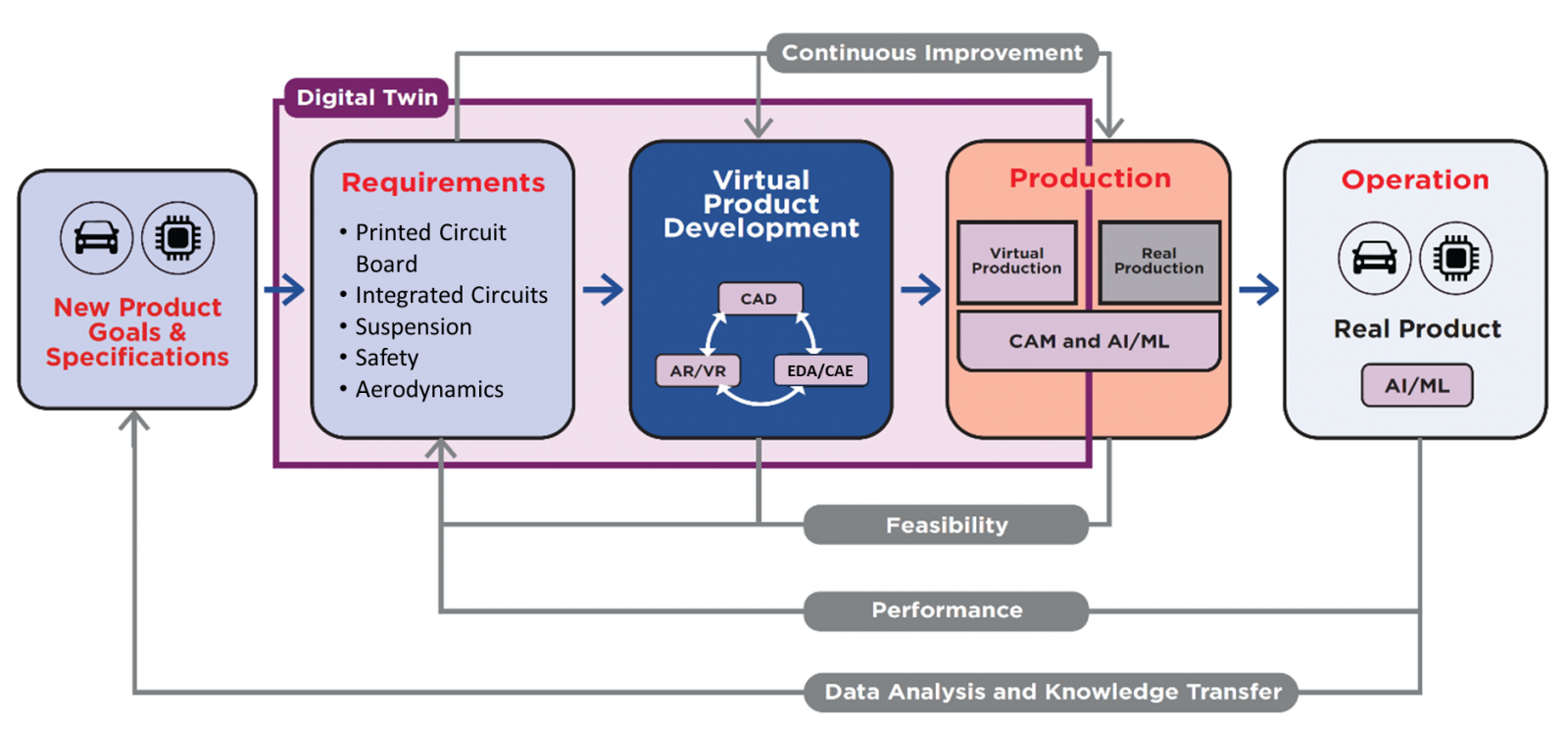
Figure 2. Digital Twin in the Automotive Industry and the use of EDA and CAE
Improved Results
With its technology partnership with AMD, Lenovo provides this flexible, end-to-end, high-performance infrastructure (Figure 3) and increases a manufacturer's ROI from EDA with:
- Accelerated Results: Lenovo systems, powered by AMD EPYC™ processors, deliver faster time-to-results for EDA tasks, enabling quicker project iterations.
- Enhanced Model Handling: These high-performance systems can manage larger and more complex simulation models, improving simulation accuracy and detail.
- Better Engineering Collaboration: Distributed engineering teams can have the correct information available to the right person at the right time, something hard to do with isolated, individual workstations.
- Energy Efficiency: Lenovo engineers design servers to help reduce power consumption and operational costs by leveraging the energy efficiency of AMD EPYC™ processors.
- Reliability and Cost Savings: Key system characteristics include high reliability, availability, and serviceability, minimizing downtime and helping lower the total cost of ownership.
- Flexible Infrastructure and Integration: Lenovo offers a flexible, pay-as-you-go model with TruScale and seamless integration with immersive manufacturing solutions (Remote Visualization, AR/VR, etc.), optimizing cost management and facilitating better product development throughout the lifecycle.
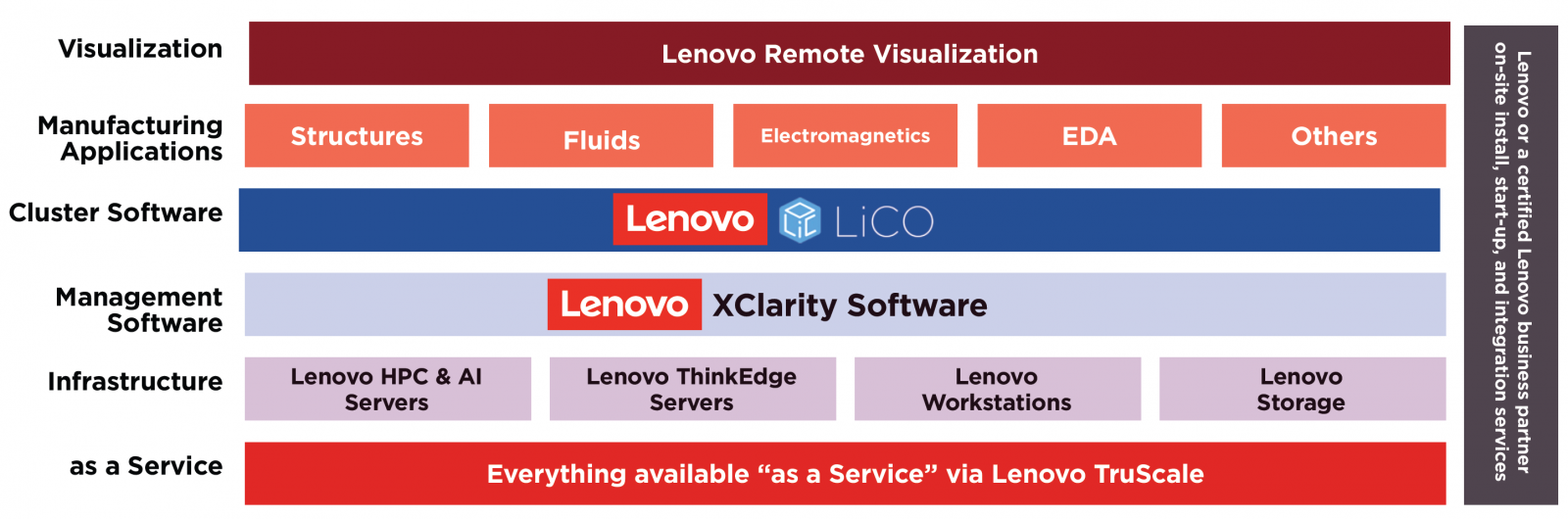
Figure 3. Lenovo's End-to-End High-Performance Infrastructure for Engineering Simulation
Read the whitepaper
To learn more about increasing the ROI from your EDA environment, download the new Lenovo whitepaper, "Raising the Bar for High-Performance Manufacturing Solutions", available from:
https://www.lenovo.com/us/en/servers-storage/alliance/amd-hpc/
Author
Patrick Moakley is the Director of Marketing for HPC & AI at Lenovo Infrastructure Solutions Group. He has over 30 years in IT sales and marketing of x86 systems at Lenovo and IBM and has a Bachelor's degree in Economics from the University of Wisconsin-Madison.
Trademarks
Lenovo and the Lenovo logo are trademarks or registered trademarks of Lenovo in the United States, other countries, or both. A current list of Lenovo trademarks is available on the Web at https://www.lenovo.com/us/en/legal/copytrade/.
The following terms are trademarks of Lenovo in the United States, other countries, or both:
Lenovo®
Other company, product, or service names may be trademarks or service marks of others.
Configure and Buy
Please select a locale


