

Top
Authors
Published
16 Nov 2023Form Number
LP1852PDF size
13 pages, 1.1 MBSubscribed to LP1852.
Thank you for your feedback.
Abstract
AMD Infinity Architecture, introduced with the 2nd Gen AMD EPYC Processors, provides the data path and control support to interconnect core complexes, memory, and I/O. Each Core Complex Die (CCD) connects to the I/O die via a dedicated high-speed Global Memory Interface (GMI) link. The socket-to-socket Infinity Fabric increases CPU-to-CPU transactional speeds by allowing multiple sockets to communicate directly through dedicated external GMI (xGMI) lanes.
AMD EPYC 9004 Series Processors support up to four xGMI links with speeds up to 32Gbps. Lenovo ThinkSystem SR665 V3 has a flexible xGMI link design allowing 1 xGMI link to be converted to additional PCIe 5.0 lanes.
This paper demonstrates how to change xGMI hardware configuration, introduces related UEFI settings, compares the performance between four xGMI links vs. three xGMI links, and provides configuration recommendations for different use cases.
This paper is suitable for customers, business partners, and sellers who wish to understand xGMI link settings and performance impact on Lenovo ThinkSystem servers SR665 V3 with AMD 4th Generations EPYC processors.
Infinity Fabric
Infinity Fabric (IF) is a proprietary AMD designed architecture that connects and facilitates data and control transfer between all components. IF is implemented in most of AMD's recent microarchitectures in their EPYC processors and other products.
In the AMD EPYC Processor, the Core Complex Dies (CCD) connect to memory, I/O, and each other through an updated I/O Die (Figure 1). Each CCD connects to the I/O die via a dedicated high-speed Global Memory Interconnect (GMI) link. The I/O die helps maintain cache coherency and additionally provides the interface to extend the infinity fabric to a potential second processor via its xGMI. AMD EPYC 9004 Series Processors support up to 4 xGMI with speeds up to 32Gbps.
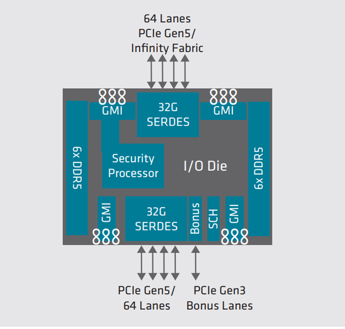
Figure 1. AMD 4th Gen EPYC processor I/O die function logical view (source: AMD)
xGMI Configurations on SR665 V3
The Lenovo ThinkSystem SR665 V3 is a 2U 2-socket server that features 4th Generation AMD EPYC processors. Figure 2 shows the architectural block diagram of the SR665 V3, showing the major components and their connections. Note that one of the xGMI links between the processors can be interchanged with two PCIe 5.0 x16 connections. These PCIe connections can be utilized for additional PCIe/NVMe support.
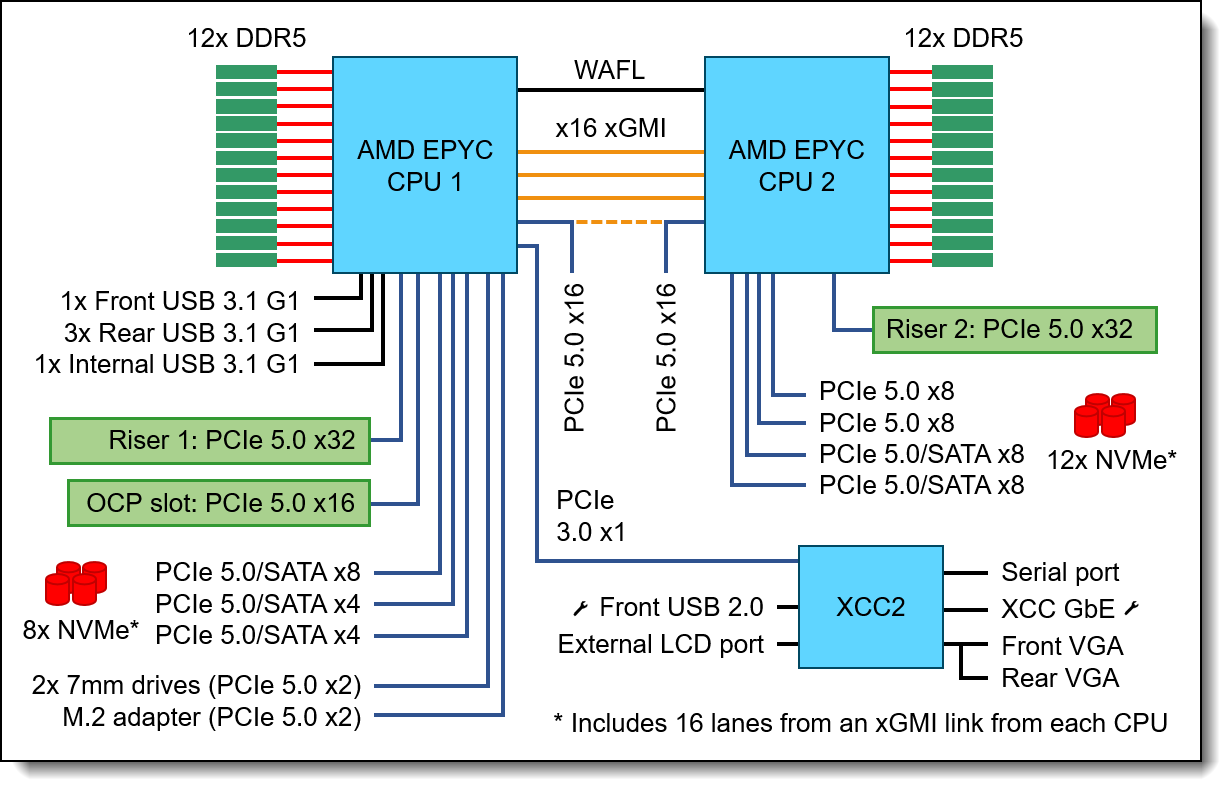
Figure 2. SR665 V3 system architectural block diagram
The cable inside the red box in Figure 3 is a 2xSwiftX8-2*SwiftX8 cable (PN SC17B23935). Installing this cable results in the 4 xGMI link configuration. Removing this cable results in the 3 xGMI link configuration. In the removed configuration, the connectors can be used to connect additional backplane to support 8 more NVMe devices.
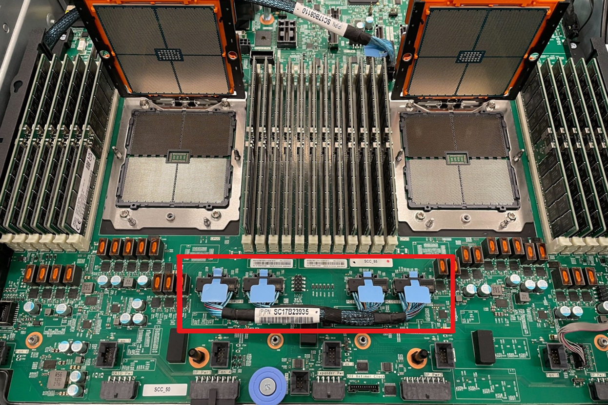
Figure 3. xGMI cable location on SR665 V3
UEFI Settings Related to xGMI
This section describes the UEFI settings used to configure xGMI.
OneCLI is a command-line tool that you can use to set these parameters. Download OneCLI from:
https://support.lenovo.com/us/en/solutions/ht116433-lenovo-xclarity-essentials-onecli-onecli
Link Speed Settings
NUMA-unaware workloads may need maximum xGMI bandwidth because of extensive cross-socket communications. NUMA-aware workloads may want to minimize xGMI speed do to not having extensive cross-socket traffic. Lowering the link speed decreases cross-socket bandwidth and increases cross-socket latency; however, lowering the link speed can also save uncore power (CPU power not consumed by the cores) to reduce overall power consumption and increase core frequency.
4-Link xGMI Max Speed:
- System setup: System Settings > Processors > 4-Link xGMI Max Speed
- OneCLI: Processors.4-LinkxGMIMaxSpeed
- Values:
- 32Gbps
- 25Gbps
- 18Gbps
- Minimum [16Gbps]
3-Link xGMI Max Speed:
- System setup: System Settings > Processors > 3-Link xGMI Max Speed
- OneCLI: Processors.3-LinkxGMIMaxSpeed
- Values:
- 32Gbps
- 25Gbps
- 18Gbps
- Minimum [16Gbps]
Link Width Settings
xGMI Dynamic Link Width Management saves power during periods of low socket-to-socket data traffic by reducing the number of active xGMI lanes per link from x16 to x8 or x4 if the xGMI links have limited traffic. Latency may increase in some scenarios involving low-bandwidth, latency-sensitive traffic as the processor transitions from a low-power xGMI state to full-power xGMI state.
Setting xGMI Force Link Width eliminates any such latency jitter. Applications that are not sensitive to both socket-to-socket bandwidth and latency can use a forced link width of x8 or x4 to save power, which can divert more power to the cores for boost.
Notes:
- xGMI Force Link Width cannot be set via System Setup (F1 on boot). You will need to use OneCLI to configure it.
- If xGMI Force Link Width Control is changed from its default of Auto, the xGMI Max Link Width will not work since the xGMI link is constantly forced to the static value.
xGMI Maximum Link Width:
- System setup: System Settings > Processors > xGMI Maximum Link Width
- OneCLI: Processors.xGMIMaximumLinkWidth
- Values:
- Auto
- x16
- x8
- x4
xGMI Force Link Width:
- System setup: Not available
- OneCLI: Processors.xGMIForceLinkWidth
- Values:
- Auto
- x16
- x8
- x4
xGMI Link Status Check
AMD offers a validation tool named AMD XIO for physical interfaces, including PCIe and xGMI. This tool can be used to verify the status of the xGMI links after they are set in UEFI.
Access to the tool: AMD XIO is only available under NDA from AMD. If you would like to use this tool, please contact AMD directly.
The following figures show the two different xGMI configurations and link status in the different operating modes.
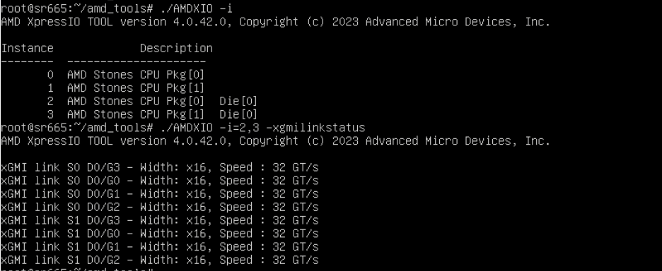
Figure 4. 4 xGMI link status in the Maximum Performance Mode
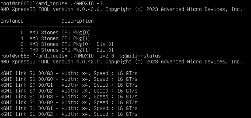
Figure 5. 4 xGMI link status in the Maximum Efficiency Mode
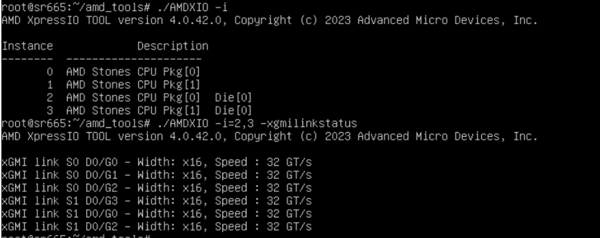
Figure 6. 3 xGMI link status in the Maximum Performance Mode
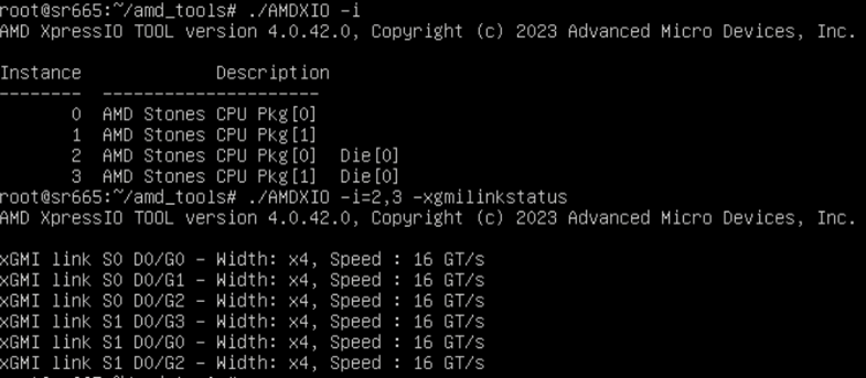
Figure 7. 3 xGMI link status in the Maximum Efficiency Mode
Theoretical Value Analysis
AMD EPYC 9004 Series Processors incorporating PCIe Gen 5 capabilities onto the I/O die, use the same physical interfaces for Infinity Fabric connections. xGMI is one such connection utilizing different protocols layered on the same PHY layer. Note that xGMI Links are bidirectional hence multiplying by two directions.
| xGMI Config | Bisection Theoretical BW |
|---|---|
| 3 links x16 32Gbps | 3 x 16 x 32Gbps / 8 x 2 directions = 384 GB/s |
| 4 links x16 32Gbps | 4 x 16 x 32Gbps / 8 x 2 directions = 512 GB/s |
| 3 links x4 16Gbps | 3 x 4 x 16Gbps /8 x 2 directions = 48 GB/s |
| 4 links x4 16Gbps | 4 x 4 x 16Gbps /8 x 2 directions = 64 GB/s |
| Memory Config | Memory Theoretical BW |
|---|---|
| 12 x 4800MHz | 12 x 4800 x 64bit / 8 = 460800 MB/s = 460.8 GB/s |
| 10 x 4800MHz | 10 x 4800 x 64bit / 8 = 384000 MB/s = 384 GB/s |
| 8 x 4800MHz | 8 x 4800 x 64bit / 8 = 307200 MB/s = 307.2 GB/s |
| 6 x 4800MHz | 6 x 4800 x 64bit / 8 = 230400 MB/s= 230.4 GB/s |
| 4 x 4800MHz | 4 x 4800 x 64bit / 8 = 153600 MB/s = 153.6 GB/s |
| 2 x 4800MHz | 2 x 4800 x 64bit / 8 = 76800 MB/s = 76.8 GB/s |
| 1 x 4800MHz | 1 x 4800 x 64bit / 8 = 38400 MB/s = 38.4 GB/s |
Four xGMI links can support a maximum theoretical bandwidth of 512 GB/s between sockets, which more than matches the maximum single socket theoretical memory bandwidth of 460.8 GB/s. This means remote memory access can flow nearly at maximum bandwidth from one CPU to another.
Three xGMI links maximum theoretical bandwidth is 384 GB/s, the same as 10 channels' maximum theoretical memory bandwidth. This means remote memory access can flow nearly at maximum bandwidth from one CPU to another when 10 or fewer DIMMs per socket.
Performance Test Benchmark
STREAM Triad is a simple, synthetic benchmark designed to measure sustainable memory bandwidth throughput. The goal is to measure the highest memory bandwidth supported by the system. STREAM Triad will be used to measure the sustained memory bandwidth of various xGMI and NUMA configurations. Unless otherwise stated, all test configurations were done using 96GB 2R RDIMMs running at 4800 MHz.
For more information about STREAM Triad, see the following web page:
http://www.cs.virginia.edu/stream/
STREAM is a NUMA-aware workload. The NUMA-aware architecture is a hardware design that separates all cores into multiple clusters where each cluster has its own local memory region and promotes working within that region; cores are still allowed to access all memory in the system. Firmware will attempt to interleave all memory channels on each quadrant of the socket (NPS4), half of the socket (NPS2), or the whole socket (NPS1) resulting in multiple nodes within the system.
Each node contains a subset of all CPUs and memory. The access speed to the main memory is determined by the location of the data relative to the CPU. Since STREAM is NUMA-aware, the application assesses data that is local to the CPU the thread is working on to get better performance. This means that there is minimal cross socket talk thus the xGMI impact is minimal.
The following table shows the stream test result of 3 xGMI link config systems and 4 xGMI link config systems in the different operating modes when NPS4. The Whole system's memory bandwidth of 3 xGMI link config system is very close to 4 xGMI link config system in the same operating mode. We can see similar behavior when NPS1&2.
| xGMI HW Config | UEFI Settings | Stream Triad (GB/s) |
|---|---|---|
| 3 links | Maximum Performance Mode NUMA Nodes per Socket = NPS4 |
742 |
| 4 links | Maximum Performance Mode NUMA Nodes per Socket = NPS4 |
744 |
| 3 links | Maximum Efficiency Mode NUMA Nodes per Socket = NPS4 |
716 |
| 4 links | Maximum Efficiency Mode NUMA Nodes per Socket = NPS4 |
715 |
The following table shows the stream memory bandwidth result when NPS0. NPS0 effectively means one NUMA node for the entire system. It is only available on a 2-socket system. Firmware will attempt to interleave all memory channels in the system. Since there are no local nodes for the application to leverage, there is far more crosstalk between sockets to transfer data on the xGMI links. The xGMI link number, speed, and width all limit the bandwidth.
The STREAM Triad test results at NPS0 show the impact of limiting those variables as the results are close to the xGMI Theoretical BW value in Table 1. Note xGMI Maximum Link Width = x16 and xGMI Max Speed = 32Gbps in the Maximum Performance Mode. We need to change the Operating Mode to Custom Mode if we want to change the variables' value.
| xGMI HW Config | UEFI Settings | Stream Triad (GB/s) |
|---|---|---|
| 3 links | Maximum Performance Mode-> Custom Mode 3-Link xGMI Max Speed = 32Gbps xGMI Maximum Link Width = x16 NUMA Nodes per Socket = NPS0 |
373 |
| 4 links | Maximum Performance Mode -> Custom Mode 3-Link xGMI Max Speed = 32Gbps xGMI Maximum Link Width = x16 NUMA Nodes per Socket = NPS0 |
491 |
| 3 links | Maximum Performance Mode -> Custom Mode 3-Link xGMI Max Speed = Minimal[16Gbps] xGMI Maximum Link Width = x4 NUMA Nodes per Socket = NPS0 |
47 |
| 4 links | Maximum Performance Mode -> Custom Mode 4-Link xGMI Max Speed = Minimal[16Gbps] xGMI Maximum Link Width = x4 NUMA Nodes per Socket = NPS0 |
63 |
Memory Latency Checker (MLC) is a tool used to measure memory latencies and bandwidth. It also provides options for local and cross-socket memory latencies and bandwidth checks.
For more information about MLC, see the following web page:
https://www.intel.com/content/www/us/en/download/736633/763324/intel-memory-latency-checker-intel-mlc.html
We use the following commands to print a local and cross-socket memory latencies/bandwidth matrix:
mlc --latency_matrix
mlc --bandwidth_matrix
The following table shows the local and cross-socket memory latency and bandwidth on the 4 xGMI config system with different xGMI link width and speed. The local node latency and bandwidth don’t impact by xGMI link status , but for the remote node bandwidth and latency, faster speed and larger width result lower latency and higher bandwidth.
| xGMI Width/Speed | Local Node Latency (ns) | Remote Node Latency (ns) | Local Node Bandwidth (GB/s) | Remote Node Bandwidth (GB/s) |
|---|---|---|---|---|
| X4 / 16 Gbps | 110.5 | 351.8 | 369.6 | 24.8 |
| X4 / 32 Gbps | 110.8 | 250.7 | 369.8 | 50.1 |
| X16 / 16 Gbps | 110.4 | 244.6 | 369.8 | 90.6 |
| X16 / 32 Gbps | 110.4 | 199.1 | 370.2 | 152.2 |
The following table shows the result of the 3 xGMI config system, and we can get the same conclusion.
| xGMI Width/Speed | Local Node Latency (ns) | Remote Node Latency (ns) | Local Node Bandwidth (GB/s) | Remote Node Bandwidth (GB/s) |
|---|---|---|---|---|
| X4 / 16 Gbps | 111.2 | 348.8 | 369.8 | 18.6 |
| X4 / 32 Gbps | 110.8 | 245.6 | 370.3 | 37.5 |
| X16 / 16 Gbps | 111.2 | 243.6 | 370.3 | 68.9 |
| X16 / 32 Gbps | 110.4 | 196.9 | 370.2 | 116.3 |
Figures 8-9 are the remote node latency/bandwidth comparison between 3 xGMI links system and 4 xGMI links system. We can see the remote node latency is very close, but 4 xGMI has much better remote node bandwidth than 3 xGMI, and the ratio is close to 4:3, which is the same as number of links compared. Besides the number of xGMI links, the Remote node bandwidth is also scalable with the xGMI width and speed.
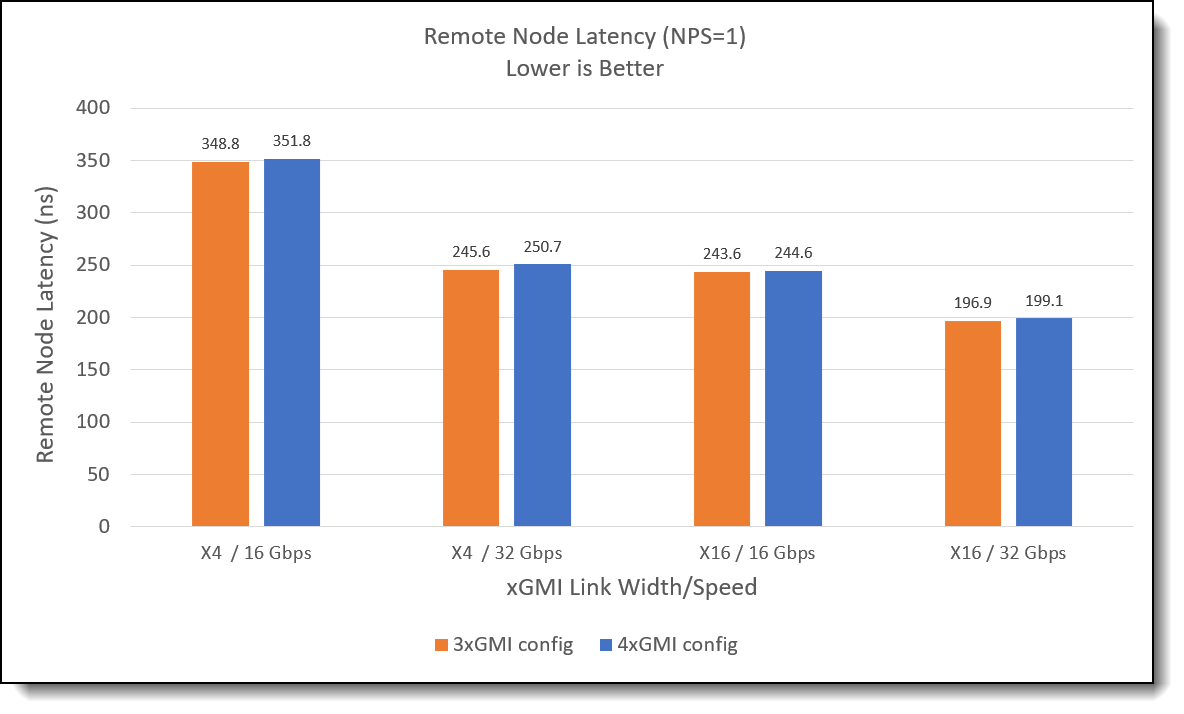
Figure 8. Remote Node Latency compares between 3 xGMI links and 4 xGMI links
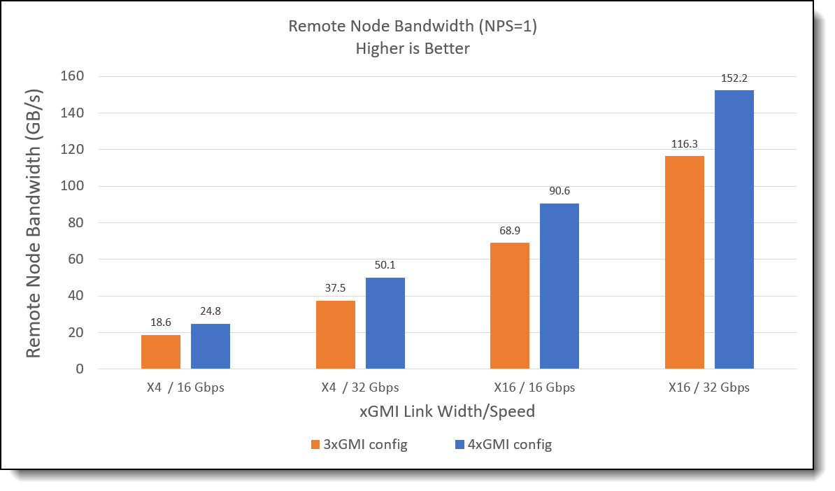
Figure 9. Remote Node Bandwidth compares between 3 xGMI links and 4 xGMI links
Summary
The ThinkSystem SR665 V3 has flexible xGMI inter-processor links allowing one link to be converted to two x16 PCIe 5.0 connections, which can provide more PCIe connections for greater PCIe/NVMe support.
Four xGMI links maximum theoretical bandwidth is greater than 12 Channels 4800MHz DDR5 BW, which means remote memory access can flow nearly at maximum bandwidth from one CPU to another. Three xGMI links may be acceptable for NUMA-aware workloads or reduced memory population.
xGMI link speed and width are configurable in the UEFI. For NUMA-aware workloads, reduced link speed and width can save uncore power to reduce overall power consumption and divert more power to the cores for increased core frequency.
For those NUMA-unaware workloads, when accessing the memory attached directly to CPU 0, CPU 1 must cross the xGMI link between the two sockets. This access is “non-uniform”, CPU 0 will access this memory faster than CPU 1 because of the distance between two sockets. The xGMI link number, speed, and width will impact the overall performance at that time.
Authors
Peter Xu is a Systems Performance Verification Engineer in the Lenovo Infrastructure Solutions Group Performance Laboratory in Morrisville, NC, USA. His current role includes CPU, Memory, and PCIe subsystem analysis and performance validation against functional specifications and vendor targets. Peter holds a Bachelor of Electronic and Information Engineering and a Master of Electronic Science and Technology, both from Hangzhou Dianzi University.
Redwan Rahman is a Systems Performance Verification Engineer in the Lenovo Infrastructure Solutions Group Performance Laboratory in Morrisville, NC, USA. His current role includes CPU, Memory, and PCIe subsystem analysis and performance validation against functional specifications and vendor targets. Redwan holds a Bachelor of Science in Computer Engineering from University of Massachusetts Amherst.
Related product families
Product families related to this document are the following:
Trademarks
Lenovo and the Lenovo logo are trademarks or registered trademarks of Lenovo in the United States, other countries, or both. A current list of Lenovo trademarks is available on the Web at https://www.lenovo.com/us/en/legal/copytrade/.
The following terms are trademarks of Lenovo in the United States, other countries, or both:
Lenovo®
ThinkSystem®
X4
Other company, product, or service names may be trademarks or service marks of others.
Configure and Buy
Please select a locale


